


TOP > Report & Column > The Forefront of Space Science > 2006 > Encouraging Analog Integrated Circuitry
![]()

Introduction Space missions have been driven partly by advances in semiconductor technology. Small- or medium-scale integrated circuits (hereinafter, referred to as “ICs”) built to perform functions required by a spacecraft often become too huge to put in the spacecraft. In addition, the electric power consumption required by the function may impose an extreme burden on the spacecraft. With introduction of large-scale ICs, it becomes possible to realize highly functional and complex systems for spacecraft operable in a space environment. These systems, however, have been realized mainly by technological advances in digital circuitry such as high-integration, high-functionality and low power-consumption. On the other hand, the use of analog electronic circuits for the processing of sensor signals, etc., has not spread as far compared to digital ICs. This is because analog circuitry requires exquisite and creative design - contrary to expectations - and, accordingly, design standardization is difficult. Furthermore, there is limited manpower specializing in analog design. Thus, analog-IC use in space systems is scarce and still remains at a level where they provide relatively small-scale elements such as operational amplifiers or single functions even when they are relatively large-scale ICs such as A-to-D and D-to-A converters. The incorporation of large-scale analog circuit systems which combine these individual elements into future spacecraft will not only constrain space missions in terms of space, weight and power consumption, but also become an obstacle to the development of highly functional spacecraft. Open-IP When building complex systems, one approach is to build up the element subsystems in layers. Adopting this approach and utilizing existing, proven circuit blocks, I am attempting, as my research theme, to set up and spread a scheme that allows us to develop large-scale and complex digital/analog mixed-mounting ICs efficiently in a short time while maintaining a certain level of integrity. More specifically, we are accumulating the knowledge of experts as “intellectual property (IP)” and making use of the IP “Open.” IP is available to aid design and development and feedback from the actual design and development sides will be accumulated in the IP. This is the aim of the “Open-IP.” In the Open-IP, aiming at the so-called Deep Submicron CMOS (*1) process (i.e., MOS transistors with gate lengths under 0.35 μm or 0.25 μm), we decided to draw circuit topologies (i.e., constituent elements) from conventional circuit design and then make them public together with typical circuit parameters such as (W, L). Further, by standardizing the interface conditions between respective circuit elements, we construct systems without internal inconsistency. By using the IP developed with this approach, we can remove the hurdles to analog circuit design and also improve integrity in operation for the resulting configured circuits. In addition, we plan to enrich the IP by adding appropriate and timely circuit topologies, that are devised and proven in the process of circuit design using public 0pen IP. With these approaches, the spiral development and expansion of the Open-IP can be pursued. For this purpose, it becomes important for us to participate in and cooperate with individual trial developments in order to actually transfer complementary know-how and obtain new IP. ISAS of JAXA is developing a system in which pixelated silicon or cadmium telluride is used as a sensor to discern energy and observe imaging in the X-ray or γ-ray region. As part of the development, a prototype pixel-type ASIC (*2) structured with 4,096 channels is being developed using Open-IP. The prototype chip incorporates the following in its 200 μm x 200 μm pixel area: charging amplifiers; shaping amplifiers; peak-hold circuits; analog multiplexes; test-pulse circuits; digital-control circuits; etc. We aim to achieve a low power characteristic of 150 μW per pixel and noise level equivalent to under 100 electrons. This performance is achieved by a multilateral design approach including bias-circuit stabilization, power-sensitivity minimization, and semiconductor-process selection. Fig. 1 shows the layout of a single pixel.Connection with a radiation sensor is made by bumps (fine metal projections) figure. The first chip was designed and fabricated by the 0.25μm CMOS process of the TSMC (Taiwan Semiconductor Manufacturing Company) and its basic function was confirmed. The second trial production is now under preparation. 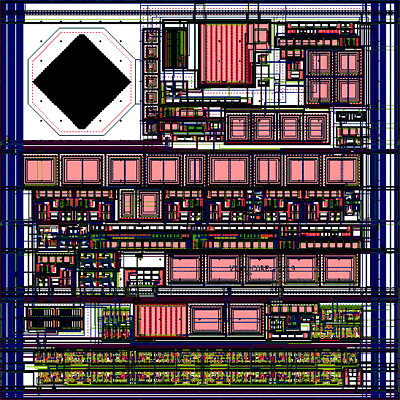
(*1) CMOS Abbreviation of Complementary Metal-Oxide Semiconductor. The conductivity of the semiconductor surface of MOS (Metal-Oxide Semiconductor) can be controlled by gate electrodes. An MOS that has two types of transistors that are complementary in response to voltage imposed on the gate is called a CMOS. (*2) ASIC Abbreviation of Application Specific Integrated Circuit. ASIC has been developed to provide the most suitable IC for application technology, even though production volume is small.
|
||||