


TOP > Report & Column > The Forefront of Space Science > 2011 > Development of Space-Application Semiconductor Integrated Circuits Space/Commercial Common-Use Strategy
![]()
Completion of the most advanced space-application LSI, system-on-chip (SoC) MHI completed the most advanced system-on-chip (SoC) by utilizing the cell libraries and multi-job run approach we had created in our project. Following the SoC prototype production in 2007, we have continuously improved the design and conducted radiation exposure tests. The SoC was finally completed this year. As shown in Fig. 1, there are space-application MPUs satisfying our target specification of more than 100MIPS processing speed. They are currently imported from overseas but extremely expensive. Power consumption of such MPUs is a few W, not meeting our target. The world-standard radiation hardness SoC we developed is small, 15mm x 10mm in chip size, with 32bit MPU of 100MIPS processing speed and implements both memory and space-wire interface on a single chip. Thus the SoC is not only superior in function and performance, it is also boasts power consumption of less than 1W. We also realized a low price making it competitive even in the commercial market, and believe that we have successfully produced the world-class common-use processor fully made in Japan. The SoC is slated to be onboard the next astronomical satellite. Furthermore, it is under consideration for use in MHI's commercial mass-production equipment. Following the R&D of the space-application LSI above, we recently started R&D on ultra-small implementation of LSIs using a cutting-edge microfabrication technology called Micro Electro-Mechanical System (MEMS) (Fig. 3). If this challenge is successful, we will be able to produce high-function space LSIs and make them ultra-small suitable for installation on satellites. 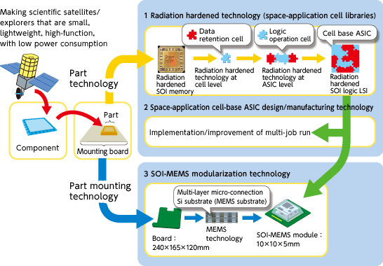
Our project has come to fruition 11 years after it was first proposed. The R&D results during the period were summarized in 19 papers and published in the U.S.'s IEEE, the most prestigious academic journal in the world in the field of radiation exposure effect of semiconductors. We were also ranked in the top ten of "Success Cases of Japan's Industry, Government, and Academia Partnership R&D," as assessed by the National Institute of Advanced Industrial Science and Technology (AIST) last year. This year we were also awarded the JAXA Performance Prize. At the time when we launched this project, few people believed that ISAS could develop space-application MPUs necessary for scientific satellites. Nonetheless, professors and researchers at ISAS appreciated the value of our research, and the administrative staff in charge of budget control, contracts, accounting, and public relations have continually supported us. Taking this opportunity, we would like to extend our sincere tanks to all of them. Kazuyuki Hirose / Hirobumi Saito
|
||||||