


TOP > Report & Column > The Forefront of Space Science > 2011 > Development of Space-Application Semiconductor Integrated Circuits Space/Commercial Common-Use Strategy
![]()

Design technology The cell-base ASIC method was adopted as a design methodology of the LSI. This method is to carry out layout design by combining memory cells and logic cells, which are standard circuit blocks prepared in advance as a cell library. By applying measures to enhance radiation hardness to each memory cell, there is no need to consider the impact of radiation in circuit design. This allows anyone to design freely, even non-specialists in space LSI. By making our cell libraries available to commercial users, they could use the libraries to design radiation-hardened LSIs for high-reliability commercial equipment as well as freely designing space-application LSIs required for a wide range of missions. Thus, this helps us collaborate with commercial field. With common use, we can also obtain LSIs at a lower cost. Circuit technology To increase radiation hardness, we adopted a method to add feedback resistance (R)/capacitance (C) to LSIs. The triple (i.e. majority) redundancy approach - a general correction method for errors caused by a Single Event Upset - forces us to increase chip size by about three times. The feedback resistance/capacitance addition approach, which suppresses propagation of transient pulses with an RC filter, can inhibit increase in chip size. In fact, since we adopted the Silicon-on-Insulator (SOI) process discussed below, we successfully limited the size increase, to a relatively small 1.3 times (approximate). The approach we adopted, however, lowers operation speed. To minimize the reduction, we needed to perform a 3D device-circuit mixed simulation and radiation exposure test to optimize values and positions of the inserted feedback resistance/capacitance. As a result, we could also limited the drop in operation speed to 30%. Manufacturing process technology By utilizing the commercial mass-production process, we can manufacture LSIs cheaper than the conventional space-specific process. We employed the most cutting-edge commercial SOI process (0.2µ fully depleted SOI process), which is expected to improve operation speed and decrease power consumption of LSIs. Since SOI has, as known well, no parasitic thyristor structure, it does not cause Single Event Latchup that could possibly lead to eternal failure. As for susceptibility to a Single Event Upset, the SOI process has the advantage of reducing collection charges. This is because the embedded silicon dioxide film, a SOI specific structure, prevents the electron-holes (generated on the LSI silicon substrate due to radiation) from intruding into channel areas. Meanwhile, since parasitic capacitance is small, SOI has one drawback in that the potential inside LSI fluctuates greatly in response to minute collection charges. Therefore, to increase radiation hardness, circuit technology using simulation is indispensable. Develop space-application LSIs at a low cost by multi-job run approach Full development started in 2002 using the three technologies above. We actively performed 3D device circuit mixed simulation and radiation exposure test to predict the radiation hardness. Then, we designed and manufactured the basic memory cell. We finally succeeded in developing a memory called SRAM using commercial technology. The memory is not only Single Event Latchup free, but also the most resistant in the world to Single Event Upset. The Upset occurrence frequency of our memory is once per 270 years in geosynchronous orbit. Subsequently, we established the cell libraries necessary for LSI design over 2003 to 2005. Thus, we created an environment where anyone can design space-application LSI of 300 gates scale in the 5mm x 5mm area. From 2005, we began research into a high-speed communication controller and processor needed to design high-performance LSIs. At that time, we also provided our cell libraries to satellite makers and universities that had not joined our common-use strategy. We also tried the multi-job run approach where the manufacturing cost was shared by joint manufacturing our LSIs and their design LSIs. In this way, we demonstrated that even a third party was able to develop space-application LSI at a low cost (Fig. 2). 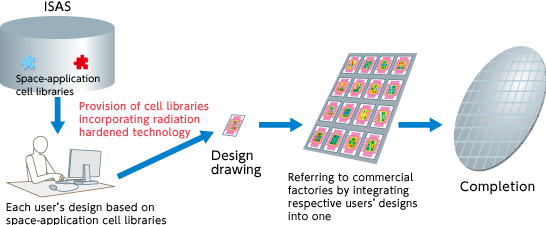
|
||||||