


TOP > Report & Column > The Forefront of Space Science > 2006 > Encouraging Analog Integrated Circuitry
![]()

SOI-CMOS use, however, was very limited for a while. Since the maturation speed of commercial bulk CMOS technology was too fast, SOI-CMOS was unable to match bulk CMOS in performance. However, the saturation trend in the technological growth curve (i.e., delay from Moore's Law) was observed with bulk CMOS in the 1990s and, as a means to overcome this saturation, SOI was revived. It was realized that, in addition to its well-known zero-latch-up advantage, SOI technology exceeds the most advanced submicron bulk CMOS in performance of operation frequency, power consumption, leakage current, degree of integration, etc. In this way, SOI technology can be seen to preempt so-called post-scaling technology (i.e., technology that advances performance without relying on miniaturization). Still, it remains uncertain that the circuit configuration adopted in Open-IP can apply to SOI in an as-is condition. In order to confirm this, we fabricated prototypes of a preamplifier and its peripheral circuitry used in radiation measurement, which are, among analog circuit elements, most sensitive to characteristics inherent in the semiconductor process. Fig. 3 shows a circuit diagram of the amplifier element as an example. Full-depletion-type SOI process is used as the semiconductor process. This process has many advantages in analog-circuit applications. For example, since carriers are completely eliminated from the silicon area just under the gates, abnormal undulations in the I-V curve are mitigated compared to the partial-depletion-type SOI of conventional technology. Within its small chip size of 2.4 mm x 2.4 mm, the prototype circuit contains 10 signal channels in total of the following three circuits including their variations: one where signals decay according to CR’s time constant; one where signals go back to the baseline linearly in place of time constant; and one high-speed trans-impedance circuit. The first circuit is a conventional charge-sensitive type amplifier circuit that can easily evaluate electronic noise such as 1/f noise. The second features excellent proportional relation of input charge and output signal width even if input signals are saturated, and provision of one solution for restriction of power voltage. The third converts current signal to voltage. This circuit uses MOS transistors biased by low current as a feedback element and is appropriate for high frequency application. 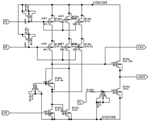
Conclusion In order to enhance the performance and reliability of electronic circuits used for space systems, ISAS is striving to expand practical application cases by simplifying design based on actual application cases, and is persevering in semiconductor technology R&D with an eye to the future. The former will be achieved by developing the Open-IP approach, and the latter by producing mature technology using the most advanced techniques such as the SOI process. (Kazuhiro IKEDA)
|
||||