TOP > Report & Column > The Forefront of Space Science > 2006 > Encouraging Analog Integrated Circuitry
![]()

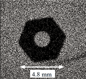
Osaka University is also developing a CCD readout system for X-ray astronomy. CCD exerts excellent performance in signal-to-noise ratio, but has the weakness of relatively inferior readout time. Thus, in order to shorten the readout time, we conducted an attempt to provide multiple output ports in a CCD chip which are readout using a custom-made ASIC. This CCD readout chip requires a noise-filter circuit, comprising integrating circuit and hold circuit, and a Wilkinson-type A/D converter circuit using 12-bit Gray-code counter for each port. Further, the University intends to deliver a noise level under 10-electrons by utilizing double correlated sampling. Fig. 2 shows an X-ray image taken by this IC. By extending the Open-IP, Osaka University has also initiated prototype production of a signal processing system using Δ∑ converter. In the experimental implementation of the Open-IP scheme, the IP-development spiral has already begun to rise sharply. Apart from JAXA, IP development is spreading through other projects such as: a readout circuit for an imaging-type aerogel detector and a TAC (time-to-amplitude converter) circuit for a TOP (time-of-propagation) detector with the purpose of particle identification in radiation detector for the B-factory experiment, and a pixel-type amplifier array for a 3-D detector to monitor colliding points for the ILC (International Linear Collider) project. 
Toward high reliability The practical application of ICs for space systems is not just being realized by efforts to make them highly functional. This is because ICs are exposed to harsh cosmic radiation, extremes of temperature, and temperature variations in space. It is also important to maintain their reliability throughout long-duration missions. To this end, we initiated study on the possibility to build analog IC using SOI (*3) technology. The application of SOI to digital circuits has already begun at JAXA, including ISAS. The U.S. has been developing SOI technology since around 1960 mainly for military and space applications, because it eliminates latch-up troubles and greatly reduces the single-event effect. These features are realized because each transistor in SOI is completely separated by silicon dioxide and also separated from the substrate. Latch-up is a phenomenon where excess current runs continuously as long as the switch is turned off. This is caused by a PNPN structure that forms parasitically in bulk CMOS and functions as a thyristor. It can be fatal for space systems. (*3) SOI Abbreviation of Silicon On Insulator, a type of wafer for IC fabrication with a single silicon crystal formed on the insulation layer. Applications in high-speed digital circuits or high-frequency analog circuits are expanding.
|
||||


