


TOP > Report & Column > The Forefront of Space Science > 2007 > Quality Assessment of Semiconductor Substrates for Solar Cells Using Photoluminescence - Identify Microscopic Distribution of Defects in Less Than One Second -
![]()

Booming solar-cell market Because of rising interest in environmental and energy issues in recent years, solar photovoltaics are attracting a lot of attention as a sustainable, clean energy. Along with this trend, the production of solar cells shows a rapid, consistent growth at an annual growth rate of over 30%. This in turn brings a new problem: a shortage of silicon (Si), the cell material. For terrestrial applications, multicrystalline Si solar cells, which are inexpensive and boast high-efficiency in photoelectric conversion, dominate the market with an over 60% share. If conventional single-crystalline Si cells are included, total share of the crystalline Si solar cells accounts for up to 90%. The remainder comprises thin film- or compound-base cells. While these cell types make up only a small share, they are important as the next-generation solar cells. In particular, highly efficient gallium arsenide (GaAs)-base multi-junction cells and copper indium selenide (CIS or CuInSe2)-base cells with an exceptionally high radiation tolerance are most suitable for space applications. These cells are installed on recent advanced satellites. Strongly desired quality-evaluation technology As a result of the explosive increase in demand for solar cells, the production of high-quality solar cells becomes the foremost issue. If cell efficiency could be improved, the cell area could be reduced enabling cost reductions and lower demand for material. For space applications, this could reduce the weight of cell modules. Thus, improvement in efficiency is very important. The efficiency of current solar cells has not yet reached its theoretical limitation, leaving room for various improvements. In order to create high-quality solar cells, inspection technology is required to identify what factors degrade quality, where they exist and when they have an effect. Specifically, it is essential to evaluate quality precisely at the micron level in each cell manufacturing process: from ingot or block level to substrate, cell, and module. An inspection speed within a second is also required to check huge numbers of test samples. Further, to avoid that evaluation process affects characteristics of test samples or disturbs productivity of cells, non-destructive/non-contact method is expected without any special pretreatment of cells. Cells are usually evaluated for their electrical characteristics such as current-voltage properties, but this approach is only possible at cell level. It is impossible to perform examination with high-spatial resolution to pinpoint where defects exist within the cell. There are techniques to evaluate solar cells at substrate level prior to cell fabrication, such as the microwave photoconductive decay method and surface photovoltage method. These methods are lacking, however, because of their long measuring time (tens of minutes per substrate) and insufficient spatial resolution (several millimeters). Thus, the traditional methods cannot fulfill the requirements of the current solar-cell industry. An innovative evaluation technology is urgently required. In an attempt to satisfy such requirements, we have developed a new evaluation technology that aids the creation of high-quality solar cells. Development of the photoluminescence imaging method Our laboratory is working on semiconductor quality assessment using “photoluminescence (PL).” When light with more photon energy than band gap is irradiated on semiconductors, an excess of electron-hole pairs are produced along with absorption of the light. The light generated when the pairs recombine is called PL. As you may know, when black light is shed on a fluorescent agent, it emits unique light. This is a familiar example of PL. The quality of the semiconductors is directly correlated with the intensity of PL. Therefore, by observing the intensity distribution of PL on a sample surface, we can characterize the quality of semiconductors two-dimensionally with high-resolution. The method is very simple. All that is required is to irradiate light on a test piece and detect light emitted from it. The method is both non-destructive and non-contact. Moreover, it enables quality assessment at both substrate and cell levels without any special pretreatment. In the past, PL intensity distribution was assessed by a technique called the “PL mapping method,” wherein lasers were irradiated on a test sample to measure PL intensity point by point by scanning the sample in the XY direction. This method, however, takes too much time so we developed the new “PL imaging method.” The new approach is very simple. We illuminate homogeneous light on the entire surface of a test piece and take photographs of the PL image. A high-power LED array is used for a light source and the photograph is taken by a cooled CCD camera with high sensitivity in near-infrared region. Figure 1 shows outline of the equipment. Because it is compact and portable, the equipment can be installed easily in solar-cell production lines. With the development of this equipment, it became possible to perform quality evaluation of surface-treated Si substrates or cells with high-spatial resolution of one million pixels and a short measuring time of less than a second per sample. 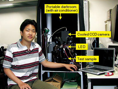
|
||||||